my Internships
Internships have significantly enriched my college life by providing invaluable real-world experience that directly complements my academic studies. They've allowed me to apply theoretical concepts learned in lectures to practical challenges, solidifying my understanding and revealing the direct relevance of my coursework.


Intel Sponsored Internship In Semiconductors And Microelectronics
Overview
Intel Sponsored Summer Internship Consist Of:
Semiconductors And Microelectronics.
Cleanroom Experience.
Micro-Credential Certificate in Semiconductor Processing.
The OASiS Micro-Credential Certificate.
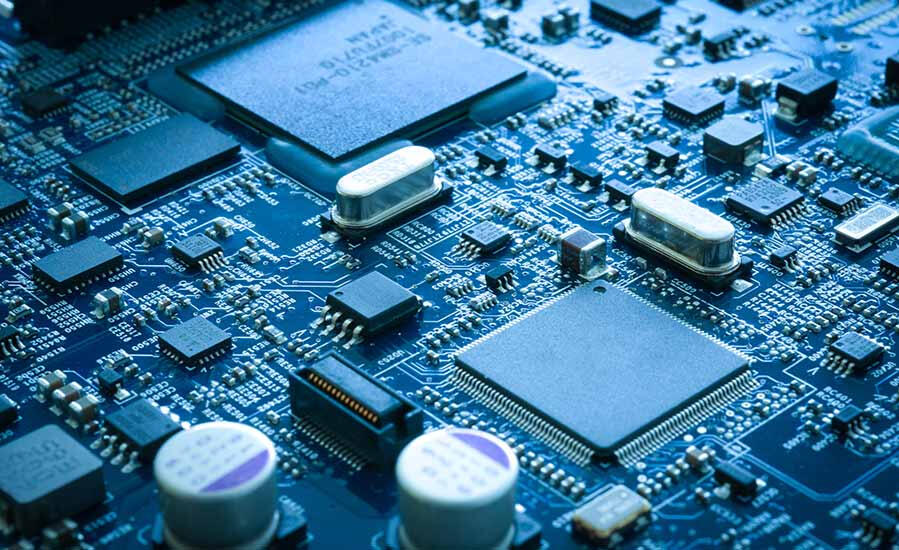
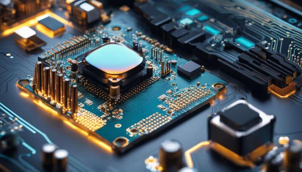
Printed Circuit Board (PCB)
What Drives Me For The Program
My journey into electrical engineering has been profoundly shaped by my growing interest in semiconductors and microelectronics. This field, at the heart of modern technology, fascinates me with its intricate processes of fabricating devices at the nanoscale, enabling everything from advanced computing to sophisticated sensors. Understanding the fundamental physics behind material properties, the complex lithography techniques, and the challenges of integrating billions of transistors onto a single chip drives my academic pursuits and future career aspirations.
To further my practical understanding, gaining cleanroom experience has been invaluable, offering a firsthand look at the meticulously controlled environments essential for semiconductor manufacturing. Complementing this, pursuing a Micro-Credential Certificate in Semiconductor Processing has provided specialized knowledge in fabrication techniques, quality control, and the operational intricacies of a fab. These experiences bridge the gap between theoretical coursework and real-world application, equipping me with the hands-on skills and industry insights necessary to contribute meaningfully to the ever-evolving landscape of microelectronics.
Software:
Cadence
KiCad
Intel Quartus Prime
Vivado


CMOS Designs And Schematics

Printed Circuit Board Designs (PCB)
Printed Circuit Board (PCB) designs are absolutely fundamental in microelectronics, serving as the physical backbone for integrated circuits and other miniature components. In this highly miniaturized realm, PCB design goes far beyond simple component interconnection; it's a critical engineering discipline that directly impacts device performance, reliability, and form factor.
Challenges include managing signal integrity at high frequencies, dissipating heat from densely packed components, and ensuring power distribution networks are stable. Advanced PCB designs for microelectronics often utilize High-Density Interconnect (HDI) technologies, featuring microvias and extremely fine traces to maximize component density within shrinking footprints, ultimately enabling the compact and powerful electronic devices we rely on today.
Building A Four Circuit Design Using The Arduino Uno 3 on A PCB
Designing a Printed Circuit Board (PCB) to build a 7-segment display integrated with Keypad, RGB and a Buzzer with an Arduino Uno 3 involves translating the breadboard prototype into a robust, compact, and permanent solution. This process requires careful consideration of component placement to minimize trace lengths and prevent signal interference, especially for the display segments and current-limiting resistors. Routing traces efficiently, often utilizing multiple layers for complex designs, ensures proper electrical connectivity while adhering to manufacturing constraints like trace width and spacing.
Schematic Diagram Of The Design

Photos For The Designs
Front View Of The PCB

Side View

Back Side Of The PCB


Full Project On GitHub
Click on the link below:
Watch Full Video Of The Project


ACCESS TO CAREERS IN ENGINEERING AND SCIENCES (ACES)
ACES 2024
University Of California
Irvine, USA

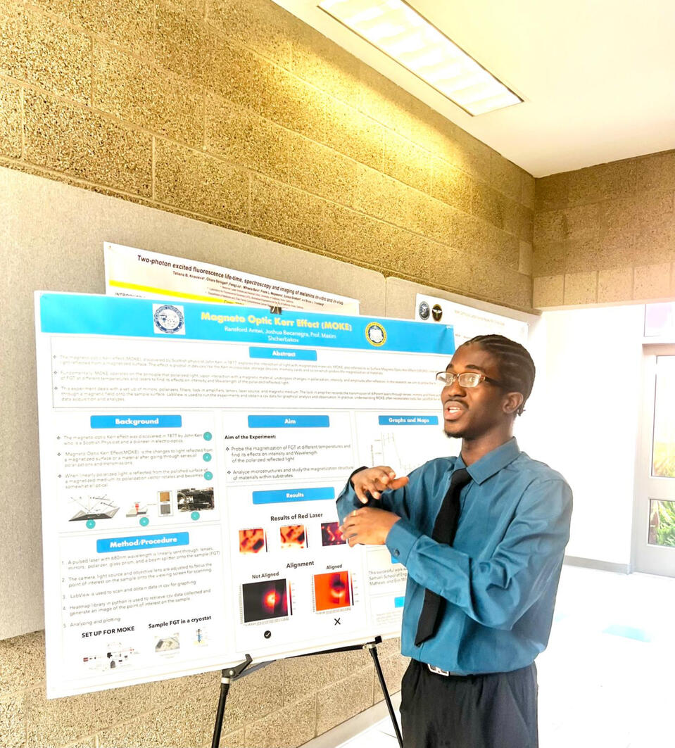
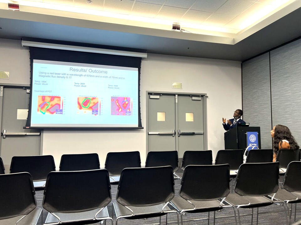
Contribute to cutting-edge research on Magneto Optic Kerr Effect (MOKE) and explore the fascinating world of semiconductor magnetization.
Learn how to use lasers to hit a 2D semiconductor and analyze some properties such as polarization, curie point and hysteresis to change in temperature.
About MOKE
This project focuses on the Magneto-Optic Kerr Effect in
2D ferromagnetic materials (FGT-Iron, Germanium,
Tellurium). By utilizing pulsed lasers, we investigated
the influence of temperature on the magnetic
properties of FGT. Our goal was to manipulate the
material's magnetization using lightThis research has the potential to
revolutionize the semiconductor industry by enabling
the development of ultra-small memory devices.
Additionally, it has implications for advanced
microscopy techniques, allowing us to visualize
microscopic structures in materials.
Project Focus
Magneto Optic Kerr Effect (MOKE)
Study of semiconductor magnetization
Analysis of magnetic domains and microstructures
Responsibilities
Modeling the rotation of the major axis of polarization
Working with different colors of lasers
Analyzing reflections from 2D semiconductor materials
Utilizing LabView and Python for data analysis and modeling
Pictures from Internship